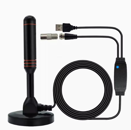
PCB onboard antenna connection module
Introduction
When it comes to wireless communication, the antenna plays a significant role in ensuring reliable and stable signal transmission. The use of PCB (printed circuit board) antenna offers several advantages such as low cost, compact size, and ease of integration. This article focuses on how to connect a PCB antenna to a module and optimize its performance.
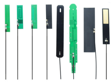
Design Considerations
The choice of antenna type and its placement on the PCB board is critical for achieving optimal RF (radio frequency) performance. Antenna gain, radiation pattern, impedance matching, and power handling capacity are some of the key parameters that must be evaluated during the design process.
The PCB antenna design process involves the following steps:
1. Antenna selection: Select an appropriate antenna type based on the frequency band of operation, required gain, and radiation pattern.
2. Antenna placement: Determine the optimal location on the PCB board to mount the antenna based on the device's mechanical and electrical requirements.
3. Impedance matching: To ensure maximum power transfer between the module and the antenna, it is essential to match their impedance values. This can be done using matching networks such as inductors, capacitors, or transmission lines.
4. Ground plane design: The PCB board's ground plane can affect the antenna's radiation pattern and efficiency. It is necessary to ensure that the ground plane is well connected, located far from the antenna, and free from any obstacles.
Connecting PCB Antenna to a Module
Connecting the PCB antenna to the module requires proper handling to avoid any RF losses or damage. The following steps outline the process of connecting a PCB antenna to a module:
1. Determine the connector type: Select a connector that is compatible with the module and the antenna's connector type. Common connector types used for module-antenna connections include u.fl, SMA, RP-SMA, and MMCX.
2. Soldering: Solder the connector to the PCB board using the recommended soldering techniques, such as reflow or wave soldering. It is essential to ensure that the solder joint is well-formed, has no voids, and does not exceed the recommended temperature and duration.
3. Testing the connection: Test the connection by measuring the RF parameters such as return loss and insertion loss. Any deviations from the desired values should be rectified by adjusting the matching network or the placement of the antenna.
Conclusion
PCB antenna design and connection to a module require knowledge and expertise in RF engineering to achieve optimal performance. By following the steps outlined in this article, device manufacturers can ensure reliable and stable wireless communication in their products. Always consult an RF expert for guidance on antenna design and integration to avoid any costly mistakes.
